| CPC H01L 21/76897 (2013.01) [H01L 21/76807 (2013.01); H01L 21/76816 (2013.01); H01L 21/76837 (2013.01); H01L 21/76877 (2013.01); H01L 23/5226 (2013.01); H01L 23/5283 (2013.01)] | 13 Claims |

|
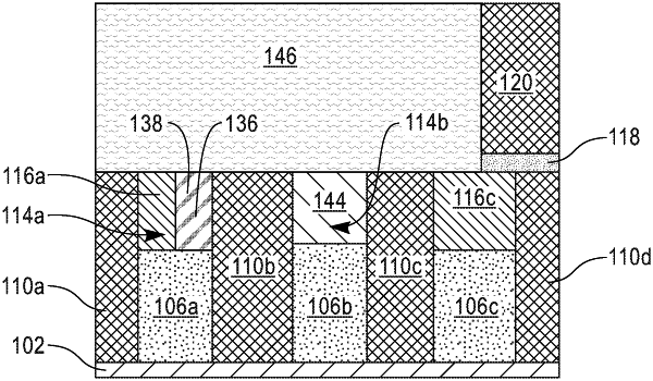
1. A semiconductor structure, comprising:
a first lower conductive line laterally insulated by a first lower dielectric region and a second lower dielectric region;
a lower level via region above the first lower conductive line, comprising:
a dielectric blocking material contacting the first lower dielectric region; and
a spacer material laterally between and contacting both: i) the second lower dielectric region and ii) the dielectric blocking material; and
an upper conductive line directly contacting top surfaces of the dielectric blocking material, the spacer material, and the first lower dielectric region.
|
|
8. A semiconductor structure, comprising:
a first lower level via region over a first lower level conductive line laterally insulated by a first lower dielectric region and a second lower dielectric region, comprising:
a spacer region comprising a spacer material contacting the second lower dielectric region; and
a first dielectric blocking material laterally between and contacting both i) the first lower dielectric region and ii) the spacer region; and
a second lower level via region over a second lower level conductive line comprising a conductive via electrically coupling the second lower level conductive line to an upper conductive line, wherein the upper conductive line directly contacts top surfaces of the first dielectric blocking material, the spacer material, and the first lower dielectric region.
|