| CPC H01L 21/3212 (2013.01) [H01L 21/02183 (2013.01); H01L 21/32139 (2013.01); H01L 21/762 (2013.01); H01L 23/00 (2013.01); H01L 23/5226 (2013.01)] | 20 Claims |

|
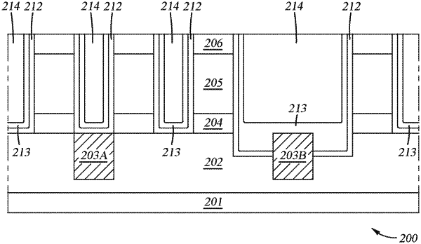
1. A layer stack, comprising:
a first dielectric layer of dielectric material;
a plurality of metal contacts comprising a deep metal contact, the plurality of metal contacts at least partially in the first dielectric layer;
a first etch stop layer disposed over and in contact with the first dielectric layer;
a second dielectric layer over the first etch stop layer;
one or more narrow trenches in the first etch stop layer and the second dielectric layer, a depth of the one or more narrow trenches defined by the first etch stop layer; and
a modified deep trench in the first etch stop layer, the second dielectric layer, and the first dielectric layer, the modified deep trench over the deep metal contact, the modified deep trench having a deeper depth than a depth of at least one of the narrow trenches, the modified deep trench extending partially into the dielectric material of the first dielectric layer.
|