| CPC H01L 21/0217 (2013.01) [C23C 16/345 (2013.01); C23C 16/56 (2013.01); H01L 21/02123 (2013.01); H01L 21/0234 (2013.01); H01L 21/02345 (2013.01); H10B 41/27 (2023.02); H10B 41/35 (2023.02); H10B 43/35 (2023.02); H01L 21/0228 (2013.01); H10B 43/27 (2023.02)] | 19 Claims |

|
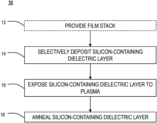
1. A processing method comprising:
selectively depositing a silicon-containing dielectric layer in a recessed region of a film stack, the film stack comprising alternating layers of a first material layer and a second material layer and having a memory hole extending through the film stack;
exposing the silicon-containing dielectric layer to a high-density plasma at a temperature less than or equal to 500° C. and at a pressure less than 1 Torr; and
annealing the silicon-containing dielectric layer at a temperature greater than 800° C. to provide a silicon-containing dielectric film having a wet etch rate of less than 4 Å/min.
|