| CPC H01J 37/32174 (2013.01) [C23C 16/24 (2013.01); C23C 16/509 (2013.01); H01J 37/32697 (2013.01); H01L 21/32055 (2013.01); H01L 21/32137 (2013.01); H01L 21/32138 (2013.01); H01L 29/66545 (2013.01)] | 18 Claims |

|
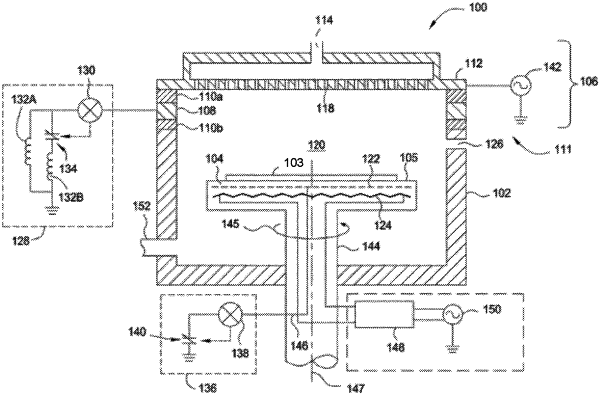
1. A processing method comprising:
forming a plasma of a silicon-containing precursor;
depositing a flowable film on a semiconductor substrate with plasma effluents of the silicon-containing precursor, wherein the semiconductor substrate is housed in a processing region of a semiconductor processing chamber, wherein the semiconductor substrate defines a feature within the semiconductor substrate, and wherein the processing region is at least partially defined between a faceplate and a substrate support on which the semiconductor substrate is seated;
forming a treatment plasma within the processing region of the semiconductor processing chamber, wherein the treatment plasma is formed at a first power level from a first power source, and wherein a second power level is applied to the substrate support from a second power source; and
densifying the flowable film within the feature defined within the semiconductor substrate with plasma effluents of the treatment plasma;
wherein the second power source is operated in a pulsing mode at a pulsing frequency of less than or about 1 kHz.
|