| CPC G09G 3/3607 (2013.01) [G06V 40/1318 (2022.01); G09G 2354/00 (2013.01)] | 4 Claims |

|
1. A liquid crystal display device with an optical sensor comprising:
a display panel comprising a first substrate, a second substrate facing the first substrate, and a liquid crystal layer located between the first substrate and the second substrate; and
a driver IC,
the display panel comprising:
a first signal line supplying video signals to a first sub-pixel corresponding to red, a second signal line supplying video signals to a second sub-pixel corresponding to green, and a third signal line supplying video signals to a third sub-pixel corresponding to blue;
an optical sensor comprising a photoelectric conversion element that outputs a detection signal in response to light incident from the liquid crystal layer side; and
a sensor signal line connected to the optical sensor and transmitting the detection signal to the driver IC, wherein
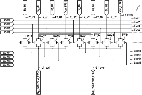
one first wiring line drawn from one terminal of the driver IC is connected to four switching elements,
three of the four switching elements are electrically connected to one of the first signal line, the second signal line, and the third signal line, respectively,
one of the four switching elements, which is different from the three switching elements, is electrically connected to the sensor signal line,
two of the four switching elements electrically connected to the first signal line and the third signal line share one semiconductor layer,
the four switching elements are each provided with an n-type semiconductor and a p-type semiconductor,
n-type semiconductors of two of the four switching elements electrically connected to the first signal line and the third signal line share one first semiconductor layer, and
p-type semiconductors of two of the four switching elements electrically connected to the first signal line and the third signal line share one second semiconductor layer.
|