| CPC G09G 3/3233 (2013.01) [H10K 59/1213 (2023.02); H10K 59/1216 (2023.02); H10K 59/124 (2023.02); H10K 59/131 (2023.02); G09G 2300/0819 (2013.01); G09G 2300/0842 (2013.01); G09G 2300/0861 (2013.01)] | 25 Claims |

|
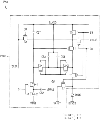
1. A display device comprising:
a light emitting diode;
a driving transistor configured to transmit driving current to the light emitting diode;
a bias transistor including an input terminal electrically connected to a bias voltage line;
a first light emission control transistor including an output terminal electrically connected to an input terminal of the driving transistor, and a gate electrode configured to receive a light emission control signal;
a second light emission control transistor including an input terminal electrically connected to an output terminal of the driving transistor, and a gate electrode configured to receive the light emission control signal;
a bias bridge electrode electrically in contact with each of an output terminal of the bias transistor and the input terminal of the driving transistor;
a first light emission control bridge electrode configured to receive the light emission control signal, defining the gate electrode of the first light emission control transistor and the gate electrode of the second light emission control transistor, and spaced apart from the bias bridge electrode when viewed in a plan view throughout a pixel circuit.
|