| CPC G07F 17/3248 (2013.01) [A63F 1/06 (2013.01); A63F 3/00157 (2013.01); G01B 11/0608 (2013.01); G06T 7/60 (2013.01); G07F 17/3206 (2013.01); G07F 17/3209 (2013.01); G07F 17/322 (2013.01); G07F 17/3241 (2013.01); G07F 17/3293 (2013.01); A63F 2009/2435 (2013.01); A63F 2009/2489 (2013.01); G06T 2207/10024 (2013.01); G06T 2207/30232 (2013.01); G06T 2207/30242 (2013.01); H04N 7/181 (2013.01)] | 18 Claims |

|
1. A system comprising:
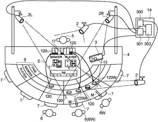
a game table having a chip tray and a plurality of placement areas arranged vertically and horizontally for placement of chips;
a first camera configured to generate a first image of a chip stack comprising one or more chips positioned in the plurality of placement areas, the first camera configured to capture the chip stack from diagonally above to generate the first image;
a second camera, different from the first camera, configured to generate a second image of the chip stack positioned in the plurality of placement areas, the second camera configured to capture the chip stack from diagonally above to generate the second image; and
a management control device configured to use deep learning techniques to perform image analysis for the first image and the second image to determine, for the same chip stack included in the first image and the second image:
a placement area of the plurality of placement areas where the chip stack is located,
a number of chips included in the chip stack, and
a type of chips included in the chip stack,
wherein the first camera is configured to capture a plurality of chip stacks placed in the same placement area or in adjacent placement areas, and
wherein the first camera and the second camera is configured to capture images of the same chip stacks from different directions, whereby if a portion of one or more chips comprising the chip stack is not visible due to a blind spot in either of the first image or the second image, the management control device is configured to, based on the first image and the second image, determine, for each chip stack of the plurality of chip stacks:
the placement area in which the chip stack is placed,
a number of chips included in the chip stack, and
a type of chips included in the chip stack.
|