| CPC G06K 19/02 (2013.01) [G06K 19/07722 (2013.01)] | 20 Claims |

|
1. A chipcard comprising:
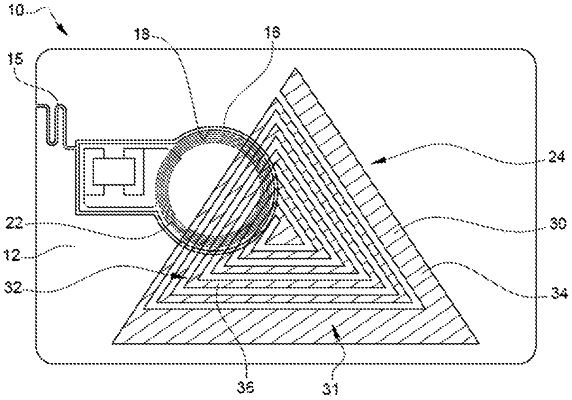
a card body formed by at least one dielectric layer and at least one metal layer superposed on the dielectric layer, the at least one metal layer including a cavity passing through its thickness and having an outline, the at least one metal layer further including a slit passing through its thickness and extending from the cavity to an edge of the card body;
an antenna extending in a plane of the cavity of the at least one metal layer;
at least one metal label at least partially covering the cavity and the antenna, the at least one metal label being fixed onto one of faces of the chipcard, the at least one metal label having a second metal layer, the second metal layer including a pattern represented by etched metal lines,
wherein the pattern of the second metal layer has a first part formed by first etched metal lines delimiting at least one zone that is at least partially of metal, and a second part composed of second etched metal lines forming only open loops,
wherein each second etched metal line of the second part of the pattern prolongs a first etched metal line of the first part of the pattern, such that the second part of the pattern forms a continuity of the first part of the pattern to form the pattern in its entirety, and
wherein the at least one metal label is positioned such that only the second part of the pattern is disposed opposite the antenna.
|