US 12,141,088 B2
Cascade communications between FPGA tiles
Daniel Pugh, Los Gatos, CA (US); Raymond Nijssen, San Jose, CA (US); Michael Philip Fitton, Menlo Park, CA (US); and Marcel Van der Goot, Pasadena, CA (US)
Assigned to Achronix Semiconductor Corporation, Santa Clara, CA (US)
Filed by Achronix Semiconductor Corporation, Santa Clara, CA (US)
Filed on Jun. 13, 2023, as Appl. No. 18/209,092.
Application 18/209,092 is a continuation of application No. 17/675,549, filed on Feb. 18, 2022, granted, now 11,734,216.
Application 17/675,549 is a continuation of application No. 16/656,685, filed on Oct. 18, 2019, granted, now 11,288,220.
Prior Publication US 2023/0325334 A1, Oct. 12, 2023
This patent is subject to a terminal disclaimer.
Int. Cl. G06F 13/40 (2006.01)
CPC G06F 13/4027 (2013.01) 20 Claims
OG exemplary drawing
 
1. A circuit comprising:
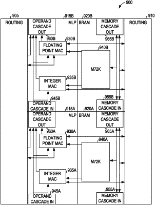
a first tile of a field programmable gate array (FPGA) comprising a first multiply and accumulate (MAC) circuit and a first memory circuit, the first memory circuit coupled to a connection fabric of the FPGA to receive a read address, an input block address, and a mask, the first memory circuit configured to:
generate a modified block address based on a block address of the first memory circuit and the mask; and
access data based on the modified block address matching the input block address; and
a second tile of the FPGA coupled to the first tile by a communication connection that does not use the connection fabric to receive the read address from the first tile.