| CPC G06F 11/1004 (2013.01) | 20 Claims |

|
1. An integrated circuit component comprising:
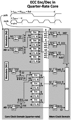
a host interface to receive a host command and write data, the write data including first and second component data values;
a memory interface; and
control circuitry, responsive to the host command, to:
generate one or more error correction codes based on the first and second component data values;
output the first component data value via the memory interface for storage within a first subset of memory ICs within a memory subsystem; and
output the second component data value together with the one or more error correction codes via the memory interface for storage within a second subset of the memory ICs within the memory subsystem;
wherein:
the memory interface comprises first and second sets of output drivers, the first set of output drivers constituted by at least 8 times as many output drivers as the second set;
the control circuitry to output the first component value via the memory interface comprises circuitry to output a plurality of portions of the first component value via the first set of output drivers over N respective transmit intervals, N being an integer greater than one; and
the control circuitry to output the second component value together with the one or more error correction codes via the memory interface comprises circuitry to output a plurality of portions of the second component value and the one or more error correction codes value via the second set of output drivers over the N transmit intervals, respectively.
|