| CPC G02F 1/1368 (2013.01) [G02F 1/136286 (2013.01); H10K 59/131 (2023.02)] | 20 Claims |

|
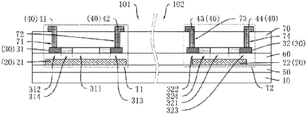
1. A display panel, wherein the display panel comprises a display region, a non-display region adjacent to the display region, a first transistor disposed in the display region, and a second transistor disposed in the non-display region, and
the display panel further comprises:
a substrate;
a first metal layer disposed on the substrate and comprising a first gate of the first transistor and a second gate of the second transistor;
an active layer disposed on a side of the first metal layer away from the substrate and comprising a first active portion of the first transistor and a second active portion of the second transistor, wherein the first active portion is located on a side of the first gate away from the substrate, and the second active portion is located on a side of the second gate away from the substrate;
a spacer layer disposed on a side of the active layer away from the first metal layer and comprising a plurality of contact holes; and
a second metal layer disposed on a side of the spacer layer away from the active layer and comprising a first source and a first drain of the first transistor, and a second source and a second drain of the second transistor, wherein the plurality of contact holes comprise a first contact hole, a second contact hole, a third contact hole and a fourth contact hole, the first source is connected to the first active portion through the first contact hole, the first drain is connected to the first active portion through the second contact hole, the second source is connected to the second active portion through the third contact hole, and the second drain is connected to the second active portion through the fourth contact hole; and
wherein both an orthographic projection of the first contact hole on the substrate and an orthographic projection of the second contact hole on the substrate are located within a coverage area of an orthographic projection of the first gate on the substrate, a boundary of the orthographic projection of the second gate on the substrate does not extend beyond a boundary of an orthographic projection of the second active portion on the substrate, and both a boundary of an orthographic projection of the third contact hole on the substrate and a boundary of an orthographic projection of the fourth contact hole on the substrate extend beyond the boundary of the orthographic projection of the second gate on the substrate.
|