| CPC G02F 1/133553 (2013.01) [G02F 1/133345 (2013.01); G02F 1/136286 (2013.01); G02F 1/1368 (2013.01); H01L 27/1248 (2013.01); H01L 27/124 (2013.01)] | 19 Claims |

|
1. A display substrate, comprising:
a first base substrate, wherein a plurality of sub-pixel regions arranged in an array are provided on the first base substrate;
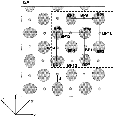
a reflective layer provided on one side of the first base substrate, wherein a surface of the reflective layer away from the first base substrate is formed to comprise a plurality of first bumps and a plurality of second bumps, and the first bumps have a size greater than that of the second bumps; and
an insulating layer provided on a side of the reflective layer facing the first base substrate, wherein a surface of the insulating layer away from the first base substrate is formed to comprise a plurality of insulating bumps, and the reflective layer is conformally formed on a side of the insulating layer away from the first base substrate, so that the reflective layer is formed to comprise the plurality of first bumps and the plurality of second bumps;
wherein in each sub-pixel region, at least one pixel electrode is provided, the reflective layer is formed of a conductive material, the reflective layer comprises a plurality of reflective parts insulated from each other, and at least one of the plurality of reflective parts is multiplexed as the pixel electrode in one of the plurality of sub-pixel regions;
wherein in each sub-pixel region, at least one transistor connected to the pixel electrode is further provided, the transistor comprises a gate electrode, a first electrode and a second electrode, and the second electrode is electrically connected to the reflective part multiplexed as the pixel electrode in the sub-pixel region;
wherein a via hole is provided in the insulating layer, and the reflective part is electrically connected to the second electrode of the transistor through the via hole; and
wherein each reflective part is electrically connected to the second electrode of the transistor in the sub-pixel region through at least two via holes arranged in a fifth direction, and an angle of the fifth direction with respect to the first direction is within a range of 15 degrees to 45 degrees.
|