| CPC G01T 1/24 (2013.01) [G01N 23/04 (2013.01); G01N 23/083 (2013.01); H01G 9/0036 (2013.01); H01G 9/2009 (2013.01); H10K 30/30 (2023.02); H10K 30/81 (2023.02); H10K 39/36 (2023.02); H10K 71/15 (2023.02); H10K 85/30 (2023.02); G01N 2223/04 (2013.01); G01N 2223/401 (2013.01); G01N 2223/50 (2013.01)] | 16 Claims |

|
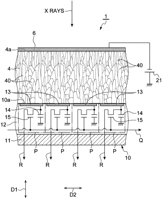
1. A radiation detector comprising:
a substrate including a first electrode portion;
a radiation absorption layer disposed on one side with respect to the substrate and configured of a plurality of perovskite crystals; and
a second electrode portion disposed on the one side with respect to the radiation absorption layer and being opposite to the first electrode portion with the radiation absorption layer interposed therebetween,
wherein each of the plurality of perovskite crystals is formed to extend with a first direction in which the first electrode portion and the second electrode portion are opposite to each other as a longitudinal direction in a region between the first electrode portion and the second electrode portion in the radiation absorption layer,
in the region between the first electrode portion and the second electrode portion, a length in the first direction of at least one of the plurality of perovskite crystals is 2 or more when a width of the perovskite crystal in a second direction perpendicular to the first direction is 1,
at least one of the first electrode portion and the second electrode portion is configured by a plurality of electrodes, and
a width of the perovskite crystal in the second direction is equal to or smaller than an arrangement pitch of the plurality of electrodes in the region between the first electrode portion and the second electrode portion.
|