| CPC G01S 7/4813 (2013.01) [G01S 17/08 (2013.01); H01L 31/0203 (2013.01); H01L 31/02164 (2013.01); H01L 31/02325 (2013.01); H01L 31/173 (2013.01); H01L 31/18 (2013.01)] | 12 Claims |

|
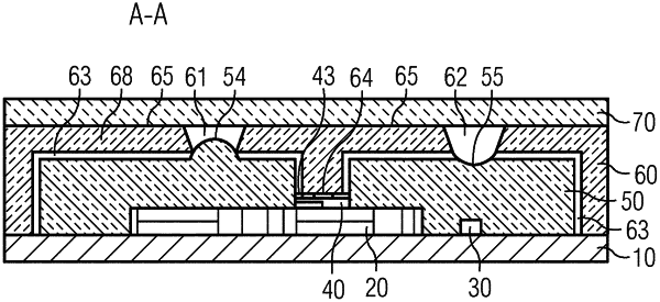
1. An optical sensor arrangement, comprising:
a substrate having a surface;
an integrated circuit comprising a first optical detector operable to detect light of a wavelength range, wherein the integrated circuit and a light emitter are mounted onto the surface, the light emitter being operable to emit light in the wavelength range, and wherein the integrated circuit and the light emitter are electrically connected to each other and to the substrate;
a light barrier formed between the first optical detector and the light emitter comprising a first optically opaque material disposed along a profile of the integrated circuit;
a mold layer encapsulating the integrated circuit the light emitter, and at least a portion of the substrate with an optically transparent material; and
a casing mounted to the light barrier made from a second optically opaque material and enclosing a hollow space between the casing and the mold layer, wherein
the mold layer comprises a first lens over the first optical detector, wherein the first lens is arranged in the optically transparent material, and
the casing comprises a first aperture aligned with the first lens, wherein the hollow space comprises at least one gap between the casing and the mold layer, and the gap is at least partially filled with a stress-decoupling elastomeric filler material, such that the first lens is mechanically decoupled from the casing.
|