| CPC G01R 33/07 (2013.01) [H10N 52/01 (2023.02)] | 32 Claims |

|
1. A device, comprising:
a Hall element having a first pair of first and second voltage sensing terminals, wherein the first and second voltage sensing terminals are located at diametrically opposed locations on the Hall element, and a second pair of third and fourth voltage sensing terminals, wherein the third and fourth voltage sensing terminals are located at diametrically opposed locations on the Hall element; and
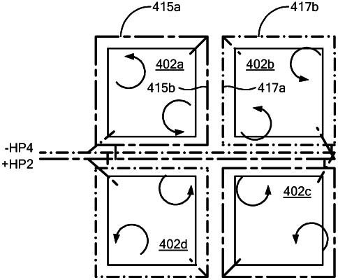
a first mirror conductive path extending around a perimeter of the Hall element in a first direction to the first voltage sensing terminal in the first pair of voltage sensing terminals and a second mirror conductive path extending around the perimeter of the Hall element in a second direction to the first voltage sensing terminal so that the first and second mirror conductive paths are on opposite sides of the Hall element and are equal and opposite to cancel inductive coupling.
|