| CPC B24B 37/22 (2013.01) [B24B 37/24 (2013.01); B24D 3/28 (2013.01); H01L 21/30625 (2013.01); C09G 1/16 (2013.01)] | 20 Claims |

|
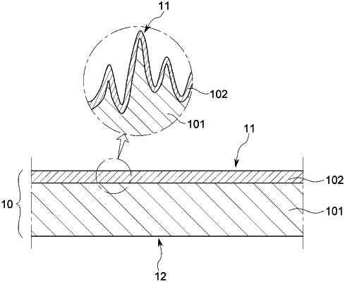
1. A polishing pad sheet comprising:
a first surface which is a polishing layer attachment surface; and
a second surface which is a rear surface of the first surface,
wherein the first surface has a value of the following Equation 1 of 4.20 to 5.50:
 where, Sv is a maximum pit height roughness value of the first surface, Sz is a maximum height roughness value of the first surface, and P is a compressibility (%) value calculated from the equation of (D1−D2)/D1×100 by collecting a specimen measuring 25 mm in width and length each from the polishing pad sheet, measuring a dial gauge in no-load condition, and then pressing with a standard weight of 85 g to measure the first thickness (D1) when 30 seconds have elapsed, and by setting up a pressure condition in which 800 g of a weight is added to the standard weight and measuring the second thickness (D2) when 3 minutes have elapsed.
|