| CPC H01L 21/0228 (2013.01) [H01L 21/02164 (2013.01); H01L 21/0217 (2013.01); H01L 21/02255 (2013.01); H01L 21/31116 (2013.01)] | 17 Claims |
|
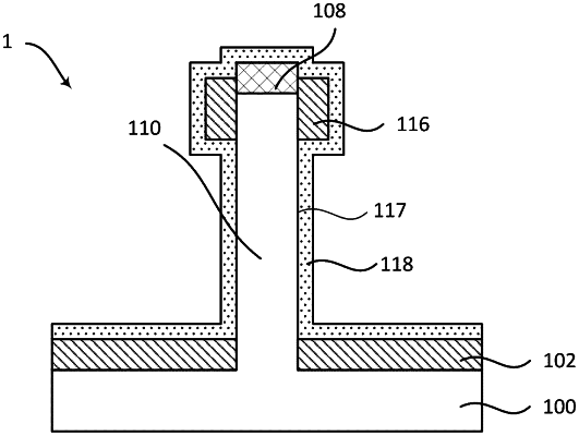
1. A method of processing a substrate, the method comprising:
loading the substrate in a processing chamber, the substrate having a raised feature with at least two sidewalls exposed on a surface of the raised feature;
depositing a first layer over the substrate adjacent to the raised feature, the first layer covering a first portion of the at least two sidewalls;
depositing a second layer over the first layer adjacent to the raised feature, the second layer covering a second portion of the at least two sidewalls, wherein the first layer and the second layer comprise different materials;
depositing a third layer over the second layer and the raised feature, the third layer covering a third portion of the at least two sidewalls and a top surface of the raised feature, wherein the second layer and the third layer comprise different materials;
performing an anisotropic dry etching that removes portions of the second layer and the third layer, a remainder of the second layer forming a second sidewall spacer and a remainder of the third layer forming a third sidewall spacer; and
performing an isotropic etching that selectively removes the second sidewall spacer to expose portions of the at least two sidewalls of the raised feature.
|