| CPC H10B 43/27 (2023.02) [H10B 43/50 (2023.02)] | 18 Claims |

|
1. A method of forming a microelectronic device, the method comprising:
forming a source structure comprising a sacrificial region positioned between a cap region and a source region;
forming pillar plugs in the source structure;
forming slit plugs in the source structure simultaneously with forming the pillar plugs;
forming a stack structure comprising a vertically alternating sequence of first material and second material over the source structure, the pillar plugs, and the slit plugs;
replacing the pillar plugs and portions of the stack structure with memory cell pillars;
forming slit openings extending through the stack structure and to the slit plugs;
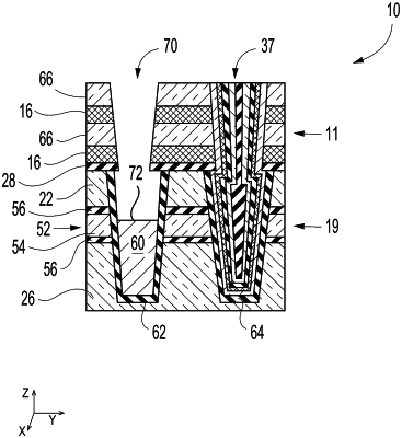
removing upper portions of the slit plugs to form extended slit openings and modified slit plugs having upper surfaces within vertical boundaries of the sacrificial region of the source structure;
forming liner material in the extended slit openings and covering the upper surfaces of the modified slit plugs;
at least partially removing portions of the liner material covering the upper surfaces of the modified slit plugs;
removing upper portions of the modified slit plugs to form further extended slit openings and further modified slit plugs having upper surfaces vertically offset from remaining portions of the liner material and positioned within the sacrificial region of the source structure;
exhuming the sacrificial material of the sacrificial region of the source structure by way of the further extended slit openings to form an open region;
filling the open region with conductive material to form a lateral conductive contact region of the source structure, the conductive material physically contacting channel material of the memory cell pillars; and
after filling the open region with conductive material, replacing the slit plugs and additional portions of the stack structure with slit structures having different configurations than the memory cell pillars.
|