| CPC H10B 43/27 (2023.02) [H10B 43/35 (2023.02)] | 16 Claims |

|
1. A method of manufacturing a semiconductor device, comprising:
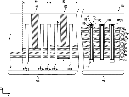
forming a stack of alternating gate layers and insulating layers over a first region and a second region of a substrate of the semiconductor device, the stack of alternating gate layers and insulating layers being of a stair-step form over the second region of the substrate;
forming a channel structure over the first region and dummy channel structures over the second region of the substrate, the dummy channel structures including a first dummy channel structure disposed through a first stair region of the stair-step form, a second dummy channel structure disposed through a second stair region of the stair-step form immediately next to the first stair region in a cross section of the semiconductor device, and a third dummy channel structure disposed at a boundary between the first stair region and the second stair region; and
forming a first contact structure over the first stair region and a second contact structure over the second stair region,
wherein the first dummy channel structure, the second dummy channel structure, the third dummy channel structure, the first contact structure, and the second contact structure are disposed along a common line in a planar view of the semiconductor device, and the first dummy channel structure, the second dummy channel structure, and the third dummy channel structure are disposed between the first contact structure and the second contact structure, the second contact structure being a contact structure that is immediately adjacent to the first contact structure along the common line in the planar view of the semiconductor.
|