| CPC H05K 1/0237 (2013.01) [H01P 3/10 (2013.01)] | 14 Claims |
|
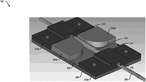
1. A surface wave launcher comprising:
a printed circuit board (PCB) comprising:
a conductor pin configured to receive a radio frequency (RF) signal; and
a ground pad;
a cylinder configured to be electrically coupled to the conductor pin and define a cylinder opening, the cylinder configured to:
receive the RF signal from the conductor pin; and
form a transition from coplanar to Goubau line structure with a ground plate structure; and
generate and propagate the surface wave;
an insulator configured to be physically positioned within at least a portion of the cylinder opening and between the cylinder and a portion of a power line, the insulator configured to mechanically isolate the cylinder from the power line and to permit the cylinder to launch the surface wave on the power line; and
the ground plate structure electrically coupled to the ground pad and configured to provide a ground reference for the conductor pin and the cylinder, the conductor pin and the cylinder physically positioned proximate the ground plate structure.
|