| CPC H05K 1/0222 (2013.01) [H01L 23/49827 (2013.01); H01L 23/552 (2013.01)] | 17 Claims |

|
1. A printed circuit board comprising:
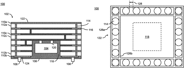
a plurality of metal layers, the plurality of metal layers comprising a first metal layer, a second metal layer, and one more intermediate metal layers, wherein the one or more intermediate metal layers are disposed between the first metal layer and the second metal layer, wherein the first metal layer comprises a metal trace;
one or more dielectric layers, wherein the one or more dielectric layers comprise a first dielectric layer disposed between the first metal layer and the one or more intermediate metal layers, wherein the one or more dielectric layers comprise a second dielectric layer disposed between the one or more intermediate metal layers and the second metal layer, wherein a first cavity is defined in the second metal layer; and
a plurality of through vias, wherein the plurality of through vias are coupled between the first metal layer and the second metal layer, wherein the plurality of through vias are arranged around a perimeter of the first cavity, wherein the metal trace couples the plurality of through vias, wherein the plurality of metal layers each comprise a plurality of annular rings, wherein the plurality of through vias are each coupled to one of the plurality of annular rings in each layer of the plurality of metal layers.
|