| CPC H01L 33/145 (2013.01) [H01L 25/0753 (2013.01); H01L 25/167 (2013.01); H01L 33/0095 (2013.01); H01L 33/0093 (2020.05); H01L 33/382 (2013.01)] | 20 Claims |

|
1. A diode array, comprising:
a substrate; and
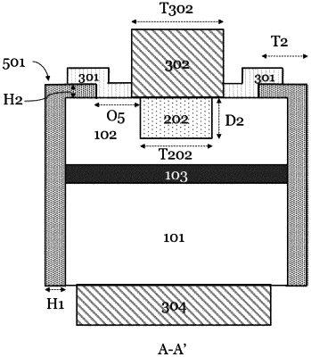
a plurality of light emitting diodes disposed on the substrate and arranged in an array, wherein each of the light emitting diodes includes a stack of functional layers comprising a first type semiconductor layer, a second type semiconductor layer, and a light emitting layer located between the first type semiconductor layer and the second type semiconductor layer,
wherein at least one of the light emitting diodes includes:
a first current blocking region abutting a vertically extending boundary of the second type semiconductor layer;
wherein, with respect to a top-down view, the first current blocking region is formed about an outer edge of the light emitting diode and an outer perimeter of the first current blocking region is equal to or less than 400 micrometers;
wherein, with respect to a cross-sectional view, an arc corner about the outer edge of the light emitting diode;
wherein, the first current blocking region covering a sidewall region has a first thickness, and the first current blocking region covering the upper surface region has a second thickness, wherein the first thickness is less than or equal to the second thickness.
|