| CPC H01L 33/0093 (2020.05) [F21S 43/14 (2018.01); F21S 43/195 (2018.01); H01L 24/05 (2013.01); H01L 24/80 (2013.01); H01L 24/94 (2013.01); H01L 27/156 (2013.01); H01L 25/167 (2013.01); H01L 2224/05571 (2013.01); H01L 2224/05647 (2013.01)] | 14 Claims |

|
1. Process for mounting a light component on a carrier, comprising:
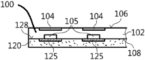
providing a light component which comprises a generally planar substrate having a first face on which a matrix-array of submillimetre-sized electroluminescent semiconductor elements are epitaxied and spatially isolated from one another in the form of a matrix;
forming at least one first electrically conductive track which comprises copper on a second face of the planar substrate of the light component which is opposite to the first face having the matrix array of submillimetre-sized electroluminescent semiconductor elements thereon;
providing a carrier;
forming at least one second electrically conductive track which comprises copper on a face of the carrier;
forming an assembly composed of the carrier and the light component by positioning the second face of the light component on said face of the carrier such that each of the first electrically conductive tracks of the light component makes contact with a respective one of the second electrically conductive tracks of the carrier;
annealing the assembly composed of the carrier and the light component at a temperature of between 200° C. and 400° C. to form a hybrid bonding connection which includes a copper-copper connection at each contact site of the first and second electrically conductive tracks, said copper-copper connection providing mechanical attachment and heat exchange between the light component and the carrier.
|