| CPC H01L 31/125 (2013.01) [H01L 31/184 (2013.01); H01L 33/0062 (2013.01)] | 2 Claims |
|
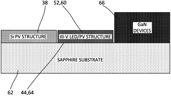
1. An optoelectronic assembly comprising:
a carrier substrate including an electrically insulating surface;
an optoelectronic structure bonded to the electrically insulating surface of the carrier substrate, the optoelectronic structure including:
a first semiconductor layer having a first conductivity type;
an intrinsic semiconductor layer on the first semiconductor layer; and
a second semiconductor layer on the intrinsic semiconductor layer and having a second conductivity type, the second conductivity type being opposite from the first conductivity type, the intrinsic semiconductor layer being between the first semiconductor layer and the second semiconductor layer;
wherein:
one of the first semiconductor layer and the second semiconductor layer is bonded to the electrically insulating surface of the carrier substrate;
the substrate comprises sapphire; and
the optoelectronic structure comprises a III-V structure including light-emitting diodes;
further comprising:
a photovoltaic structure bonded to the electrically insulating surface of the carrier substrate, the photovoltaic structure comprising:
a first doped layer comprising silicon;
an intrinsic layer comprising silicon on the first doped layer; and
a second doped layer comprising silicon and on the intrinsic layer, the second doped layer and first doped layer have opposite conductivity types; and
a region, with gallium nitride devices, on the substrate.
|