US 12,136,673 B2
Semiconductor device with self-aligned wavy contact profile and method of forming the same
Chia-Ta Yu, Hsinchu (TW); Yen-Chieh Huang, Tainan (TW); Wei-Yuan Lu, Taipei (TW); Feng-Cheng Yang, Hsinchu County (TW); and Yen-Ming Chen, Hsin-Chu (TW)
Assigned to TAIWAN SEMICONDUCTOR MANUFACTURING CO., LTD., Hsinchu (TW)
Filed by Taiwan Semiconductor Manufacturing Co., Ltd., Hsin-Chu (TW)
Filed on Aug. 10, 2023, as Appl. No. 18/447,855.
Application 17/542,810 is a division of application No. 16/656,619, filed on Oct. 18, 2019, granted, now 11,195,951, issued on Dec. 7, 2021.
Application 18/447,855 is a continuation of application No. 18/190,419, filed on Mar. 27, 2023, granted, now 11,824,121.
Application 18/190,419 is a continuation of application No. 17/542,810, filed on Dec. 6, 2021, granted, now 11,616,142, issued on Mar. 28, 2023.
Claims priority of provisional application 62/771,630, filed on Nov. 27, 2018.
Prior Publication US 2023/0387305 A1, Nov. 30, 2023
This patent is subject to a terminal disclaimer.
Int. Cl. H01L 29/78 (2006.01); H01L 21/8234 (2006.01); H01L 27/088 (2006.01); H01L 29/08 (2006.01); H01L 29/165 (2006.01)
CPC H01L 29/7848 (2013.01) [H01L 21/823418 (2013.01); H01L 21/823431 (2013.01); H01L 27/0886 (2013.01); H01L 29/0847 (2013.01); H01L 29/165 (2013.01); H01L 29/7851 (2013.01)] 20 Claims
OG exemplary drawing
 
1. A device comprising:
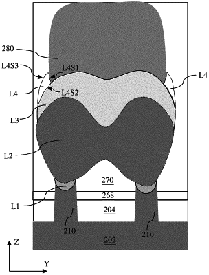
a source/drain feature disposed on a substrate, the source/drain feature including:
a first semiconductor layer, the first semiconductor layer having a non-planar top surface; and
a pentavalent silicon compound layer disposed directly on the non-planar top surface of the first semiconductor layer; and
a contact feature extending through the pentavalent silicon compound layer to the non-planar top surface of the first semiconductor layer such that the contact feature directly contacts the non-planar top surface of the first semiconductor layer and the pentavalent silicon compound layer.