| CPC H01L 29/7827 (2013.01) [H01L 29/0673 (2013.01); H01L 29/0847 (2013.01); H01L 29/1033 (2013.01); H01L 29/161 (2013.01); H01L 29/42392 (2013.01); H01L 29/66545 (2013.01); H01L 29/78696 (2013.01)] | 8 Claims |

|
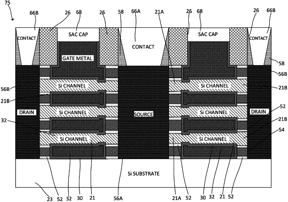
1. A gate-all-around field-effect transistor, comprising:
a vertical stack of nanosheet layers, each of the nanosheet layers including:
a source side lateral end portion,
a drain side lateral end portion having a drain side thickness, and
a channel portion between and integral with the source side lateral end portion and the drain side lateral end portion, wherein the channel portion further comprises:
an end portion integral with the source side lateral end portion and having an end portion thickness; and
a main portion integral with the drain side lateral end portion, integral with the end portion, and having a main portion thickness;
a step formed around the channel portion, between the end portion and the main portion;
wherein the end portion thickness is less than the main portion thickness; and
wherein the main portion thickness is the same as the drain side lateral end portion thickness;
a gate wrapping around and operatively associated with the nanosheet layers, wherein the gate includes a high-k gate dielectric layer and a gate metal layer;
an epitaxial source region adjoining the source side lateral end portions of the nanosheet layers and operatively associated with the nanosheet layers, wherein the source side lateral end portions of the nanosheet layers end at the epitaxial source region; and
an epitaxial drain region adjoining the drain side lateral end portions of the nanosheet layers and operatively associated with the nanosheet layers, wherein the drain side lateral end portions of the nanosheet layers end at the epitaxial drain region,
wherein the channel portion is configured for providing threshold voltage asymmetry.
|