US 12,136,670 B2
Semiconductor device having contact trenches extending from opposite sides of a semiconductor body
Markus Zundel, Egmating (DE); Andreas Meiser, Sauerlach (DE); Hans-Peter Lang, Munich (DE); Thorsten Meyer, Regensburg (DE); and Peter Irsigler, Obernberg/Inn (AT)
Assigned to Infineon Technologies AG, Neubiberg (DE)
Filed by Infineon Technologies AG, Neubiberg (DE)
Filed on May 25, 2022, as Appl. No. 17/824,198.
Application 17/824,198 is a continuation of application No. 16/235,550, filed on Dec. 28, 2018, abandoned.
Application 16/235,550 is a continuation of application No. 15/051,105, filed on Feb. 23, 2016, abandoned.
Application 15/051,105 is a continuation of application No. 13/589,717, filed on Aug. 20, 2012, granted, now 9,281,359, issued on Mar. 8, 2016.
Prior Publication US 2022/0285550 A1, Sep. 8, 2022
Int. Cl. H01L 21/74 (2006.01); H01L 21/02 (2006.01); H01L 21/762 (2006.01); H01L 21/8234 (2006.01); H01L 23/48 (2006.01); H01L 27/06 (2006.01); H01L 29/06 (2006.01); H01L 29/417 (2006.01); H01L 29/423 (2006.01); H01L 29/45 (2006.01); H01L 29/66 (2006.01); H01L 29/78 (2006.01); H01L 29/861 (2006.01); H01L 29/40 (2006.01)
CPC H01L 29/7813 (2013.01) [H01L 21/02 (2013.01); H01L 21/743 (2013.01); H01L 21/762 (2013.01); H01L 21/76224 (2013.01); H01L 21/823475 (2013.01); H01L 23/48 (2013.01); H01L 27/0629 (2013.01); H01L 27/0694 (2013.01); H01L 29/06 (2013.01); H01L 29/417 (2013.01); H01L 29/41741 (2013.01); H01L 29/41766 (2013.01); H01L 29/4236 (2013.01); H01L 29/456 (2013.01); H01L 29/66477 (2013.01); H01L 29/66727 (2013.01); H01L 29/66734 (2013.01); H01L 29/78 (2013.01); H01L 29/7803 (2013.01); H01L 29/7827 (2013.01); H01L 29/7845 (2013.01); H01L 29/861 (2013.01); H01L 21/823418 (2013.01); H01L 29/0657 (2013.01); H01L 29/407 (2013.01); H01L 2924/0002 (2013.01)] 12 Claims
OG exemplary drawing
 
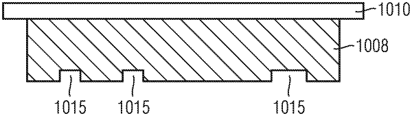
1. A method of manufacturing a semiconductor body comprising:
forming a pattern at a first side of a substrate;
forming a semiconductor layer on the first side of the substrate;
attaching the substrate and the semiconductor layer to a carrier via a surface of the semiconductor layer; and
removing the substrate from a second side opposite to the first side.