| CPC H01L 29/66969 (2013.01) [H01L 27/1207 (2013.01); H01L 27/1225 (2013.01); H01L 27/1248 (2013.01); H01L 29/78606 (2013.01); H01L 29/7869 (2013.01); H01L 21/02178 (2013.01); H01L 21/02181 (2013.01); H01L 21/02266 (2013.01); H01L 21/02554 (2013.01); H01L 21/02565 (2013.01); H01L 21/02631 (2013.01); H01L 21/8258 (2013.01); H01L 27/0629 (2013.01); H01L 27/0688 (2013.01); H01L 29/78648 (2013.01)] | 10 Claims |

|
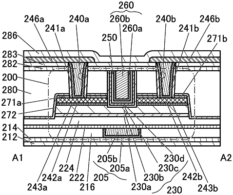
1. A method of manufacturing a semiconductor device, comprising:
forming a first insulator, a second insulator, and a third insulator sequentially;
forming a fourth insulator, a first oxide film, a second oxide film, a third oxide film, a first conductive film, a first insulating film, and a second conductive film sequentially over the third insulator;
shaping the first oxide film, the second oxide film, the third oxide film, the first conductive film, the first insulating film, and the second conductive film into island-like shapes to form a first oxide, a second oxide, a first oxide layer, a first conductive layer, a first insulating layer, and a second conductive layer, respectively;
removing the second conductive layer;
forming a fifth insulator over the fourth insulator, the first oxide, the second oxide, the first oxide layer, the first conductive layer, and the first insulating layer;
forming a sixth insulator over the fifth insulator;
forming an opening reaching the second oxide in the first oxide layer, the first conductive layer, the first insulating layer, the fifth insulator, and the sixth insulator to form a third oxide and a fourth oxide from the first oxide layer, a first conductor and a second conductor from the first conductive layer, and a seventh insulator and an eighth insulator from the first insulating layer; and
forming a fifth oxide, a ninth insulator over the fifth oxide, and a third conductor over the ninth insulator,
wherein the fifth oxide, the ninth insulator, and the third conductor are in the opening, and
wherein the fifth insulator is formed using a bias sputtering method.
|