| CPC H01L 29/42392 (2013.01) [H01L 29/0665 (2013.01); H01L 29/66477 (2013.01); H01L 29/78696 (2013.01)] | 20 Claims |
|
1. A semiconductor structure, comprising:
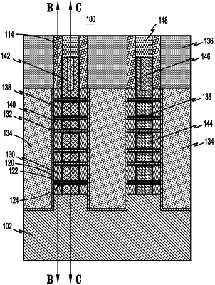
a gate structure comprising a multi-layer channel stack, the multi-layer channel stack comprising:
a first dielectric layer;
a second dielectric layer; and
a channel layer disposed between the first and second dielectric layers;
a first source/drain region disposed on a first side of the gate structure in electrical contact with a first end portion of the multi-layer channel stack; and
a second source/drain region disposed on a second side of the gate structure in electrical contact with a second end portion of the multi-layer channel stack;
wherein the multi-layer channel stack extends through an inner spacer to a contact layer electrically connecting the channel layer to the first source/drain region, the contact layer being disposed between the inner spacer and the first source/drain region, and in contact with the channel layer, the inner spacer, the first source/drain region, a bottom dielectric isolation layer, a first inter-layer dielectric layer, and a second inter-layer dielectric layer.
|