| CPC H01L 29/401 (2013.01) [H01L 21/76243 (2013.01); H01L 21/84 (2013.01); H01L 23/5226 (2013.01); H01L 23/5286 (2013.01); H01L 27/1203 (2013.01); H01L 29/165 (2013.01); H01L 29/41733 (2013.01); H01L 29/41783 (2013.01); H01L 29/42392 (2013.01); H01L 29/66439 (2013.01); H01L 29/66545 (2013.01); H01L 29/66742 (2013.01); H01L 29/78645 (2013.01)] | 16 Claims |
|
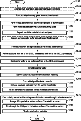
1. A method comprising:
arranging a multi-layer stack on a semiconductor substrate, wherein the multi-layer stack comprises a nanosheet stack arranged above a dielectric isolation layer;
arranging a plurality of dummy gates above the nanosheet stack;
etching through the nanosheet stack between the plurality of dummy gates to form one or more trenches;
depositing semiconductor material in the one or more trenches to form a source/drain region, wherein the source/drain region comprises a top surface and a bottom surface positioned between the top surface and the semiconductor substrate;
removing a portion of the semiconductor substrate such that the bottom surface of the source/drain region is exposed;
forming an electrical contact that extends through one or more layers to the bottom surface; and
forming a buried power rail that contacts the bottom surface through the electrical contact.
|