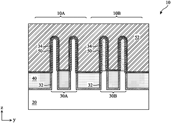
| CPC H01L 29/16 (2013.01) [H01L 21/823821 (2013.01); H01L 27/0924 (2013.01); H01L 29/66795 (2013.01); H01L 29/785 (2013.01)] | 20 Claims |

|
1. A semiconductor structure, comprising:
a semiconductor substrate;
a silicon-germanium (SiGe) fin protruding from the semiconductor substrate, wherein the SiGe fin includes a top portion having a first sidewall and a second sidewall disposed over a bottom portion having a third sidewall and a fourth sidewall, and wherein a first transition edge connecting the first sidewall to the third sidewall and a second transition edge connecting the second sidewall to the fourth sidewall each have a tapered profile extending away from the first sidewall and the second sidewall, respectively, wherein the first transition edge extends to a greater height above the substrate than the second transition edge;
isolation features disposed over the semiconductor substrate and surrounding the bottom portion of the SiGe fin;
a Si-containing layer disposed on the top portion of the SiGe fin, wherein a first portion of the Si-containing layer disposed on the first transition edge extends away from the first sidewall by a first lateral distance and a second portion of the Si-containing layer disposed on the second transition edge extends away from the second sidewall by a second lateral distance that is different from the first lateral distance, and wherein separation between outer vertical surfaces of the Si-containing layer is defined by a third lateral distance; and
a metal gate stack disposed over the Si-containing layer in a channel region of the SiGe fin.
|
|
10. A semiconductor structure, comprising:
a semiconductor substrate including a first region and a second region;
isolation structures disposed over the first region and the second region;
a first fin protruding from the semiconductor substrate in the first region, wherein the first fin includes silicon (Si) and is substantially free of germanium (Ge), wherein the first fin includes a first upper portion and a first lower portion, wherein the first upper portion has a first edge and an opposing second edge and the first lower portion has a third edge and an opposing fourth edge, wherein the first fin further includes a first transition edge tapering away from the first edge to the third edge, the first edge and the third edge being on the same side of the first fin;
a second fin protruding from the semiconductor substrate in the second region, wherein the second fin includes Si and Ge, wherein the second fin includes a second upper portion and a second lower portion, wherein the second upper portion has a fifth edge and an opposing sixth edge and the first lower portion has a seventh edge and an opposing eighth edge, wherein the second fin further includes a second transition edge tapering away from the fifth edge to the seventh edge, the fifth edge and the seventh edge being on the same side of the second fin, wherein the first transition edge extends to a different height above the substrate than the second transition edge and wherein the first fin and the second fin extend to the same height above the substrate;
a Si layer disposed over the first fin and the second fin, wherein a portion of the Si layer disposed over the first fin has a first thickness and a portion of the Si layer disposed over the second fin has a second thickness that is greater than the first thickness; and
a metal gate stack disposed over the Si layer in a channel region of the first fin and a channel region of the second fin.
|
|
17. A device comprising:
a first fin structure formed of a first semiconductor material disposed on a substrate, the first fin structure including a first upper portion and a first lower portion, wherein the first upper portion has a first edge and an opposing second edge and the first lower portion has a third edge and an opposing fourth edge, wherein the first fin structure further includes a first transition edge tapering away from the first edge to the third edge, the first edge and the third edge being on the same side of the first fin structure, wherein the first fin structure further includes a second transition edge tapering away from the second edge to the fourth edge, the second edge and the fourth edge being on the same side of the first fin structure, and wherein the first transition edge extends to a greater height above the substrate than the second transition edge;
a silicon-containing layer disposed directly on the first edge and the first transition edge;
a liner layer disposed directly on third edge of the first lower portion of the first fin structure;
a gate dielectric layer disposed directly on the silicon-containing layer; and
a gate electrode layer disposed on the gate dielectric layer.
|