| CPC H01L 29/1087 (2013.01) [H01L 21/743 (2013.01); H01L 29/0653 (2013.01); H01L 29/1095 (2013.01); H01L 29/66681 (2013.01); H01L 29/7816 (2013.01)] | 12 Claims |

|
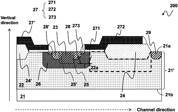
1. A high voltage device, comprising:
a semiconductor layer, which is formed on a substrate;
a well, which has a first conductivity type, and is formed in the semiconductor layer;
a body region, which has a second conductivity type, and is formed in the well;
a body contact, which has the second conductivity type, and is configured to operably serve as an electrical contact of the body region, wherein the body contact is formed in the body region;
a gate, which is formed on the semiconductor layer, wherein a part of the body region is located vertically beneath and in contact with the gate, so as to provide an inversion current channel during an ON operation of the high voltage device;
a source, which has the first conductivity type, and is formed in the body region, wherein the source is located below the gate and out of one side of the gate; and
a drain, which has the first conductivity type, and is formed in the well, wherein the drain is located below the gate at another side of the gate away from the body region, wherein a drift region is located between the drain and the body region in a channel direction and the drift region serves as a drift current channel during the ON operation of the high voltage device;
wherein a region where the body contact and the source overlaps with each other is defined as an overlap region, wherein the overlap region has the first conductivity type;
wherein the body contact has a depth extending downward from an upper surface of the semiconductor layer, wherein the depth is deeper than a depth of the source extending downward from the upper surface of the semiconductor layer, so that a part of the body contact is located vertically below the overlap region;
wherein a length of the overlap region in the channel direction is not shorter than a predetermined length, so as to suppress a parasitic bipolar junction transistor from being turned on when the high voltage device operates;
wherein the parasitic bipolar junction transistor is formed by a part of the well, a part of the body region and a part of the source;
wherein a concentration of the second conductivity type impurities of the body contact is higher than a concentration of the second conductivity type impurities of the body region.
|