US 12,136,641 B2
Imaging device and signal processing device
Jun Ogi, Tokyo (JP); Yoshiaki Tashiro, Tokyo (JP); Takahiro Toyoshima, Kanagawa (JP); Yorito Sakano, Kanagawa (JP); Yusuke Oike, Kanagawa (JP); Hongbo Zhu, Tokyo (JP); Keiichi Nakazawa, Tokyo (JP); Yukari Takeya, Kanagawa (JP); Atsushi Okuyama, Kanagawa (JP); Yasufumi Miyoshi, Kanagawa (JP); Ryosuke Matsumoto, Tokyo (JP); and Atsushi Horiuchi, Kanagawa (JP)
Assigned to Sony Semiconductor Solutions Corporation, Kanagawa (JP)
Filed by SONY SEMICONDUCTOR SOLUTIONS CORPORATION, Kanagawa (JP)
Filed on Jul. 6, 2022, as Appl. No. 17/858,688.
Application 17/858,688 is a continuation of application No. 16/987,745, filed on Aug. 7, 2020, granted, now 11,424,281.
Application 16/987,745 is a continuation of application No. 16/301,877, granted, now 10,777,597, issued on Sep. 15, 2020, previously published as PCT/JP2018/011179, filed on Mar. 20, 2018.
Claims priority of application No. 2017-055582 (JP), filed on Mar. 22, 2017; and application No. 2018-045205 (JP), filed on Mar. 13, 2018.
Prior Publication US 2022/0344386 A1, Oct. 27, 2022
Int. Cl. H01L 27/146 (2006.01); H04N 25/70 (2023.01); H01L 31/107 (2006.01)
CPC H01L 27/1463 (2013.01) [H01L 27/14623 (2013.01); H01L 27/1464 (2013.01); H01L 27/14645 (2013.01); H01L 27/14685 (2013.01); H01L 27/14689 (2013.01); H04N 25/70 (2023.01); H01L 31/107 (2013.01)] 20 Claims
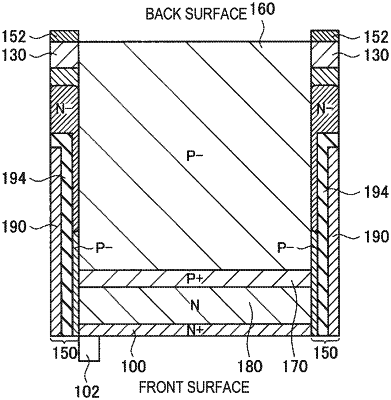
OG exemplary drawing
 
1. A light detecting device, comprising:
a first semiconductor region of a first conductivity type;
a second semiconductor region of a second conductivity type opposite to the first conductivity type;
a third semiconductor region of the first conductivity type;
a fourth semiconductor region of the second conductivity type;
a first electrode connected to the first semiconductor region;
a second electrode connected to the second semiconductor region;
a third electrode connected to the third semiconductor region;
a fourth electrode connected to the fourth semiconductor region;
a pixel separation unit including a metal region and an insulating region and disposed between the second semiconductor region and the fourth semiconductor region; and
a metal layer connected to the first and third electrodes, wherein the metal layer includes a lattice shape in a planer view.