| CPC H01L 27/1463 (2013.01) [H01L 27/14603 (2013.01); H01L 27/14612 (2013.01); H01L 27/14636 (2013.01); H01L 27/14643 (2013.01); H04N 25/77 (2023.01)] | 32 Claims |

|
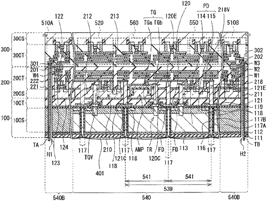
1. A solid-state imaging device, comprising:
a first semiconductor layer including a photoelectric converter and an electric charge accumulation section for each pixel, wherein the electric charge accumulation section accumulates a signal electric charge generated in the photoelectric converter;
a pixel separation section that is provided in the first semiconductor layer, wherein the pixel separation section partitions a plurality of the pixels from each other;
a second semiconductor layer that is provided with a pixel transistor and is stacked on the first semiconductor layer, wherein the pixel transistor reads the signal electric charge of the electric charge accumulation section; and
a first shared coupling section that is provided between the second semiconductor layer and the first semiconductor layer, wherein the first shared coupling section straddles the pixel separation section and is electrically coupled to a plurality of the electric charge accumulation sections;
a first substrate including the first semiconductor layer and a first wiring layer provided with the first shared coupling section;
a second substrate including the second semiconductor layer and a second wiring layer that is opposed to the first substrate with the second semiconductor layer interposed therebetween;
a third substrate that is opposed to the first substrate with the second substrate interposed therebetween, and includes a circuit that is electrically coupled to the second semiconductor layer; and
a first through electrode that electrically couples the first shared coupling section and the pixel transistor to each other, and is provided in the first substrate and the second substrate.
|