| CPC H01L 27/14629 (2013.01) [H01L 27/14607 (2013.01); H01L 27/1462 (2013.01); H01L 27/1463 (2013.01); H01L 27/1464 (2013.01); H01L 27/14685 (2013.01); H01L 31/02327 (2013.01); H01L 31/02363 (2013.01)] | 20 Claims |

|
1. A semiconductor device, comprising:
a semiconductor substrate;
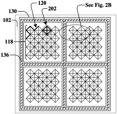
a grid structure extending from a first side of the semiconductor substrate to within the semiconductor substrate as viewed in cross-section, the grid structure including a plurality of closed-loop grid segments that adjoin one another to form the grid structure as viewed from above;
a plurality of image sensing elements disposed within the semiconductor substrate and laterally surrounded by the closed-loop grid segments, respectively; and
a plurality of protrusions arranged along the first side of the semiconductor substrate, the plurality of protrusions being disposed over a single image sensing element of the plurality of image sensing elements and being laterally surrounded by the closed-loop grid segment of the single image sensing element, the plurality of protrusions being substantially identical to one another and having a characteristic dimension, wherein an inner edge of the closed-loop grid segment facing the image sensing element is spaced apart from a peak or valley of one of the plurality of protrusions by a flat surface corresponding to a predetermined reflective length that is based on the characteristic dimension of the plurality of protrusions.
|