| CPC H01L 27/1207 (2013.01) [H01L 21/76264 (2013.01); H01L 21/76898 (2013.01); H01L 23/481 (2013.01)] | 20 Claims |

|
1. A method comprising:
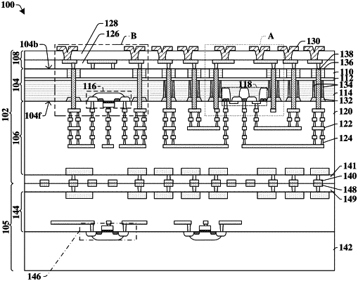
forming a first deep trench isolation (DTI) structure that extends through an active layer of a silicon-on-insulator (SOI) substrate to contact an insulator layer of the SOI substrate, wherein the SOI substrate comprises the insulator layer arranged over a base layer and the active layer arranged over the insulator layer;
forming a second DTI structure that extends through the active layer of the SOI substrate to contact the insulator layer of the SOI substrate, wherein the second DTI structure is spaced apart from the first DTI structure by the active layer;
forming a shallow trench isolation (STI) structure that extends into the active layer of the SOI substrate and that extends laterally between and contacts the first and second DTI structures;
forming a first semiconductor device on the SOI substrate, wherein the STI structure, the first DTI structure, and the second DTI structure continuously surround the first semiconductor device;
forming an interconnect structure over the first semiconductor device and the SOI substrate, wherein the interconnect structure comprises interconnect wires and interconnect vias embedded within an interconnect dielectric structure;
forming first hybrid bond layers over the interconnect structure;
bonding the first hybrid bond layers to hybrid bond layers of another integrated circuit on another substrate;
flipping the SOI substrate to thin-down the base layer of the SOI substrate;
patterning the SOI substrate to form an opening in the SOI substrate arranged between the first and second DTI structures; and
forming a through substrate via (TSV) within the opening of the SOI substrate, wherein the TSV extends completely through the SOI substrate, the STI structure, and a portion of the interconnect dielectric structure to contact an interconnect wire or interconnect via of the interconnect structure.
|