| CPC H01L 25/0657 (2013.01) [H01L 23/5256 (2013.01); H03K 5/24 (2013.01); H03K 19/20 (2013.01); H01L 2225/06513 (2013.01); H01L 2225/06527 (2013.01); H01L 2225/06541 (2013.01)] | 20 Claims |

|
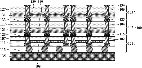
1. A method of manufacturing a semiconductor device, the method comprising:
receiving a first semiconductor device, the first semiconductor device comprising:
a first unique identifier structure;
a first electrical input; and
a first comparator comprising a first input connected to the first unique identifier structure and comprising a second input connected to the first electrical input;
a first AND gate comprising:
a fifth input connected to the first comparator; and
a sixth input connected to an external connector of the first semiconductor device;
receiving a second semiconductor device, the second semiconductor device comprising:
a second unique identifier structure different from the first unique identifier structure;
a second electrical input electrically connected to the first electrical input; and
a second comparator comprising a third input connected to the second unique identifier structure and comprising a fourth input connected to the second electrical input; and
bonding the first semiconductor device to the second semiconductor device.
|