| CPC H01L 23/562 (2013.01) [H01L 23/535 (2013.01); H01L 23/564 (2013.01); H01L 23/585 (2013.01); H01L 24/08 (2013.01); H01L 24/80 (2013.01); H01L 25/0657 (2013.01); H01L 25/18 (2013.01); H01L 25/50 (2013.01); H01L 2224/08145 (2013.01); H01L 2224/80895 (2013.01); H01L 2224/80896 (2013.01); H01L 2924/1431 (2013.01); H01L 2924/1434 (2013.01); H01L 2924/351 (2013.01)] | 18 Claims |

|
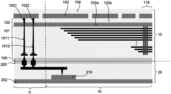
1. A memory device, comprising:
a wafer structure having a sealing region and a chip region, comprising:
a substrate;
a memory string array over a first side of the substrate in the chip region;
a first protection structure and a second protection structure on the first side of the substrate in the sealing region;
a first contact and a second contact extending through the substrate in the sealing region,
wherein the first contact is in contact with the first protection structure, and the second contact is in contact with the second protection structure; and
an insulating structure extending through the substrate in the sealing region.
|