| CPC H01L 23/5389 (2013.01) [H01L 21/4853 (2013.01); H01L 21/4857 (2013.01); H01L 21/565 (2013.01); H01L 21/78 (2013.01); H01L 23/3128 (2013.01); H01L 23/5383 (2013.01); H01L 23/5386 (2013.01); H01L 24/19 (2013.01); H01L 24/20 (2013.01); H01L 25/0652 (2013.01); H01L 25/50 (2013.01); H01L 2224/214 (2013.01); H01L 2225/06524 (2013.01); H01L 2225/06548 (2013.01); H01L 2225/06586 (2013.01)] | 31 Claims |

|
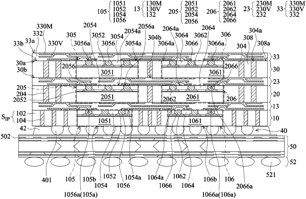
1. A semiconductor package, comprising:
a first die structure, comprising:
an interposer comprising a semiconductor substrate and through-vias penetrating through the semiconductor substrate; and
a first integrated circuit die disposed in the semiconductor substrate of the interposer;
a first redistribution structure disposed on a top surface of the semiconductor substrate of the interposer of the first die structure;
a second die structure disposed on the first redistribution structure, the second die structure comprising:
a second integrated circuit die encapsulated in an encapsulant; and
conductive pillars penetrating through the encapsulant;
a second redistribution structure disposed on the second die structure,
wherein the first integrated circuit die is electrically coupled to the second integrated circuit die through the first redistribution structure, the conductive pillars and the second redistribution structure; and
conductive connectors directly disposed on a bottom surface of the semiconductor substrate of the interposer, wherein the bottom surface of the semiconductor substrate of the interposer is coplanar with a backside surface of the first integrated circuit die, and the conductive connectors are directly connected to the through-vias of the interposer of the first die structure.
|