| CPC H01L 23/5386 (2013.01) [H01L 23/13 (2013.01); H01L 23/3675 (2013.01); H01L 23/49816 (2013.01); H01L 23/5383 (2013.01); H01L 23/5389 (2013.01); H01L 24/17 (2013.01); H01L 25/0652 (2013.01); H01L 25/16 (2013.01); H01L 24/32 (2013.01); H01L 24/73 (2013.01); H01L 2224/16145 (2013.01); H01L 2224/16227 (2013.01); H01L 2224/17181 (2013.01); H01L 2224/32245 (2013.01); H01L 2224/73253 (2013.01); H01L 2225/06513 (2013.01); H01L 2225/06517 (2013.01); H01L 2225/06541 (2013.01); H01L 2225/06589 (2013.01)] | 20 Claims |
|
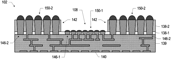
1. A microelectronic assembly, comprising:
a dielectric material having first conductive contacts at a top surface and second conductive contacts at bottom surface;
a first die above the dielectric material, the first die having a top, a bottom, a first side between the top and bottom, and a second side between the top and bottom, the second side opposite the first side, the bottom of the first die coupled to a first portion of the first conductive contacts of the dielectric material, and the first die having through-substrate vias (TSVs) therein, wherein at least one of the TSVs of the first die is coupled to a corresponding one of the first portion of conductive contacts;
a material above the dielectric material, the material having a recess therein, the recess narrowest closest to the dielectric material, wherein the first die is in the recess of the material, and the material having a first tapered sidewall laterally spaced apart from the first side of the first die, and a second tapered sidewall laterally spaced apart from the second side of the first die;
interconnects extending through the material, the interconnects coupled to a second portion of the first conductive contacts of the dielectric material;
a second die above the first die and the material, the second die coupled to the top of the first die by die-to-die interconnects, and the second die coupled to a portion of the interconnects extending through the material.
|