| CPC H01L 23/528 (2013.01) [H01L 21/6835 (2013.01); H01L 23/485 (2013.01); H01L 23/5226 (2013.01); H01L 23/53228 (2013.01); H01L 23/53233 (2013.01); H01L 23/5389 (2013.01); H01L 23/66 (2013.01); H01L 24/19 (2013.01); H01L 24/20 (2013.01); H01Q 1/2283 (2013.01); H01L 21/568 (2013.01); H01L 22/32 (2013.01); H01L 22/34 (2013.01); H01L 23/3128 (2013.01); H01L 23/3135 (2013.01); H01L 23/3171 (2013.01); H01L 24/03 (2013.01); H01L 24/06 (2013.01); H01L 24/14 (2013.01); H01L 2221/68313 (2013.01); H01L 2221/68359 (2013.01); H01L 2223/6616 (2013.01); H01L 2223/6677 (2013.01); H01L 2224/02331 (2013.01); H01L 2224/02381 (2013.01); H01L 2224/0401 (2013.01); H01L 2224/04105 (2013.01); H01L 2224/12105 (2013.01); H01L 2224/73267 (2013.01); H01L 2224/9222 (2013.01)] | 20 Claims |

|
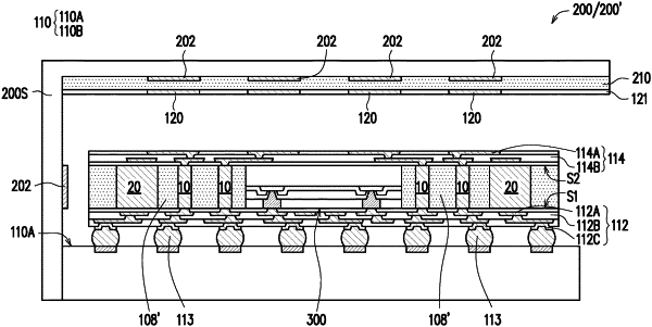
1. A structure, comprising:
a semiconductor die;
a redistribution layer disposed on the semiconductor die;
a plurality of first conductive patterns overlapped with the semiconductor die and the redistribution layer, wherein a gap or a first dielectric layer is in between the plurality of first conductive patterns and the redistribution layer
a dielectric housing covering and laterally surrounding the semiconductor die, the redistribution layer, and the plurality of first conductive patterns, wherein a gap exists in between housing side walls of the dielectric housing and the redistribution layer; and
a plurality of second conductive patterns attached on the dielectric housing and overlapped with each of the plurality of first conductive patterns, wherein both the plurality of first conductive patterns and the plurality of second conductive patterns are located on an inner surface side of the dielectric housing.
|