| CPC H01L 23/373 (2013.01) [H01L 21/565 (2013.01); H01L 23/3107 (2013.01); H01L 23/3672 (2013.01); H01L 23/4334 (2013.01)] | 9 Claims |
|
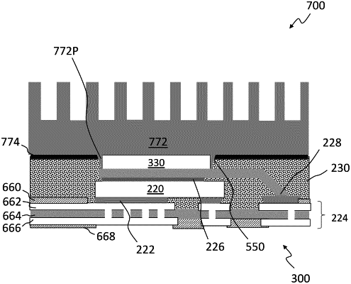
1. A chip package, comprising:
a semiconductor chip;
an elastic thermal interface material over the semiconductor chip, wherein the elastic thermal interface material is configured to transfer heat from the semiconductor chip to an outside;
a packaging material around the elastic thermal interface material and at least partially around the semiconductor chip; and
a gap between the elastic thermal interface material and the packaging material that is arranged directly above and extends along an upper surface of the semiconductor chip,
wherein the elastic thermal interface material extends above a surface level of the packaging material.
|