| CPC H01L 21/76825 (2013.01) [H01L 21/76804 (2013.01); H01L 21/76829 (2013.01); H01L 23/5226 (2013.01); H01L 23/5329 (2013.01)] | 20 Claims |

|
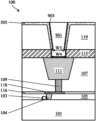
1. A method of manufacturing a semiconductor device, the method comprising:
forming an opening in a dielectric material, the opening exposing a target region of an etch stop layer overlying a conductive feature, the target region having a first etch rate with respect to an etchant;
performing a dopant implantation on a sidewall of the dielectric material and a top surface of the etch stop layer through the opening to form a first dopant implant region in the dielectric material and a second dopant implant region in the etch stop layer, wherein the second dopant implant region comprises a portion below the first dopant implant region; and
performing an etch process to remove the second dopant implant region to expose the conductive feature, wherein after removing the second dopant implant region, the etch stop layer comprises a non-doped region in physical contact with a bottom of the first dopant implant region in the dielectric material.
|
|
10. A method of manufacturing a semiconductor device, the method comprising:
depositing an etch stop layer over a first dielectric layer, the etch stop layer having a first etch rate with respect to an etchant;
depositing a second dielectric layer over the etch stop layer;
forming a first via opening through the second dielectric layer and exposing the etch stop layer;
performing an ion implantation through the first via opening, the ion implantation modifying the second dielectric layer to comprise a first doped region adjacent a sidewall of the second dielectric layer and modifying the etch stop layer to comprise a second doped region, wherein a bottom of the first doped region of the second dielectric layer connects to the second doped region of the etch stop layer;
performing a removal process with the etchant after the performing the ion implantation to remove the second doped region and form a second via opening in the etch stop layer; and
forming a metal plug in the first via opening and the second via opening, wherein the metal plug comprises a barrier layer in the first via opening and in the second via opening, wherein the barrier layer in the second via opening is in physical contact with the bottom of the first doped region of the second dielectric layer.
|
|
16. A method of manufacturing a semiconductor device, the method comprising:
forming an etch stop layer over a metallization feature;
forming an interlayer dielectric layer over the etch stop layer;
forming a first opening through the interlayer dielectric layer and exposing the etch stop layer;
performing a dopant implantation on a sidewall of the interlayer dielectric layer and a top surface of the etch stop layer through the first opening to form a first dopant implant region in the interlayer dielectric layer and a second dopant implant region in the etch stop layer, wherein a bottom of the second dopant implant region is wider than a bottom of the first opening; and
performing a removal process to remove at least a portion of the second dopant implant region and form a second opening in the etch stop layer, wherein the bottom of the second opening is wider than the bottom of the first opening.
|