| CPC H01L 21/76251 (2013.01) [H01L 21/486 (2013.01); H01L 21/6838 (2013.01); H01L 23/147 (2013.01); H01L 23/3107 (2013.01); H01L 23/3142 (2013.01); H01L 23/481 (2013.01); H01L 23/49827 (2013.01); H01L 23/5386 (2013.01); H01L 24/81 (2013.01); H01L 24/83 (2013.01); H01L 24/95 (2013.01); H01L 25/50 (2013.01); H01L 23/49816 (2013.01); H01L 23/49833 (2013.01); H01L 23/544 (2013.01); H01L 24/13 (2013.01); H01L 2221/68322 (2013.01); H01L 2223/54486 (2013.01); H01L 2224/13147 (2013.01); H01L 2224/16145 (2013.01); H01L 2224/16225 (2013.01); H01L 2224/17181 (2013.01); H01L 2224/32145 (2013.01); H01L 2224/73204 (2013.01); H01L 2224/73253 (2013.01); H01L 2224/81001 (2013.01); H01L 2224/81011 (2013.01); H01L 2224/81024 (2013.01); H01L 2224/81191 (2013.01); H01L 2224/81203 (2013.01); H01L 2224/81815 (2013.01); H01L 2224/83101 (2013.01); H01L 2224/83192 (2013.01); H01L 2224/83203 (2013.01); H01L 2224/83855 (2013.01); H01L 2224/92125 (2013.01); H01L 2924/12042 (2013.01); H01L 2924/15311 (2013.01); H01L 2924/16152 (2013.01); H01L 2924/1616 (2013.01); H01L 2924/19105 (2013.01)] | 20 Claims |

|
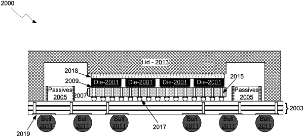
1. A semiconductor device, comprising:
an interposer comprising an interposer top side and an interposer bottom side;
a first device die comprising a first device die top side and a first device die bottom side, wherein the first device die bottom side is coupled to the interposer top side;
a second device die comprising a second device die top side and a second device die bottom side, wherein the second device die bottom side is coupled to the interposer top side; and
a third device die comprising a third device die top side and a third device die bottom side, wherein the third device die bottom side is coupled to the second device die top side.
|