| CPC H01G 4/2325 (2013.01) [H01G 4/012 (2013.01); H01G 4/30 (2013.01)] | 13 Claims |

|
1. A multilayer ceramic capacitor comprising:
a multilayer body including a plurality of stacked dielectric layers, and including a first major surface and a second major surface opposite to each other in a height direction and facing a mounting surface, a first side surface and a second side surface opposite to each other in a width direction orthogonal or substantially orthogonal to the height direction, and a first end surface and a second end surface opposite to each other in a length direction orthogonal or substantially orthogonal to the height direction and the width direction;
a first internal electrode on the plurality of dielectric layers, located inside the multilayer body, and extending to the first major surface;
a second internal electrode on the plurality of dielectric layers, located inside the multilayer body, and extending to the second major surface;
a first external electrode on the first major surface; and
a second external electrode on the second major surface; wherein
the first and second external electrodes include an underlying electrode layer including a metallic component and a glassy component, and a plating layer on the underlying electrode layer;
a difference of about 3 μm or less exists between a maximum thickness of a center portion of the first and second external electrodes and a thickness of a peripheral portion of the first and second external electrodes at a portion located on the first or second major surface and located farther inward than a peripheral end portion of the first and second external electrodes by about 10% of a length of the first and second external electrodes that connects the first and second side surfaces or the first and second end surfaces; and
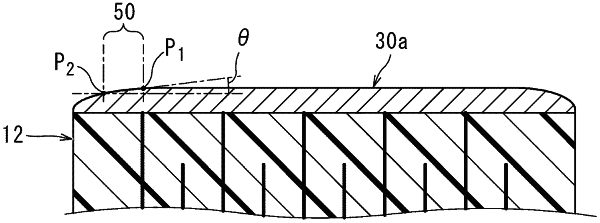
in a range of a field of view of about 50 μm square centered at a point located farther inward by about 15% than the peripheral end portion of the first or second external electrode, an angle θ of about 4 degrees or less is defined by a straight line connecting points P1 and P2 of an intersection of a surface of the first and second external electrodes and a sectional line defining the range of the field of view of about 50 μm square and a perpendicular or substantially perpendicular line to a vertical line passing through point of intersection P1 or P2.
|