| CPC G11C 7/1063 (2013.01) [G11C 7/1066 (2013.01); G11C 7/1069 (2013.01); G11C 7/1096 (2013.01); G11C 7/222 (2013.01); G11C 16/32 (2013.01); G11C 16/0483 (2013.01); G11C 16/26 (2013.01); G11C 2207/2272 (2013.01)] | 15 Claims |

|
1. A semiconductor memory device comprising:
a memory cell array;
a storing unit configured to temporarily store a plurality of data read out from the memory cell array in a plurality of storage circuits;
an output circuit configured to output data transmitted from the storing unit to an external memory controller;
a control circuit configured to control the storing unit to sequentially output data to the output circuit in response to read timing control signals received from the memory controller and in accordance with a value of a read pointer, wherein
the control circuit is configured to, in response to switching of the read timing control signals received from the memory controller:
adjust the value of the read pointer, and
control the storing unit to output data stored in one of the plurality of storage circuits corresponding to the value of the read pointer to the output circuit, and
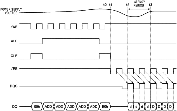
the control circuit is configured to, in response to a request for read data by the memory controller, set the value of the read pointer in accordance with a latency period during which data stored in the plurality of storage circuits are not overwritten, such that data stored in at least two of the plurality of storage circuits are output to the output circuit and transmitted from the output circuit to the memory controller as dummy data during the latency period, and are output to the output circuit and transmitted from the output circuit to the memory controller as the read data after the latency period.
|