| CPC G11C 5/10 (2013.01) [G11C 11/221 (2013.01); H01L 29/6684 (2013.01); H01L 29/78391 (2014.09); H10B 53/30 (2023.02)] | 25 Claims |
|
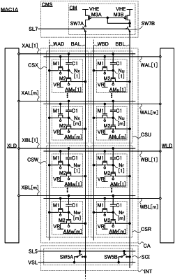
1. A semiconductor device comprising:
a first cell, a second cell, a third cell, a fourth cell, a current mirror circuit, a first wiring, a second wiring, a third wiring, and a fourth wiring,
wherein the first cell, the second cell, the third cell, and the fourth cell each comprise a first transistor, a second transistor, and a capacitor,
wherein a first terminal of the first transistor is electrically connected to a first terminal of the capacitor and a gate of the second transistor in each of the first cell, the second cell, the third cell, and the fourth cell,
wherein a first terminal of the second transistor in the first cell is electrically connected to the first wiring,
wherein a second terminal of the capacitor in the first cell is electrically connected to the third wiring,
wherein a first terminal of the second transistor in the second cell is electrically connected to the first wiring,
wherein a second terminal of the capacitor in the second cell is electrically connected to the fourth wiring,
wherein a first terminal of the second transistor in the third cell is electrically connected to the second wiring,
wherein a second terminal of the capacitor in the third cell is electrically connected to the third wiring,
wherein a first terminal of the second transistor in the fourth cell is electrically connected to the second wiring,
wherein a second terminal of the capacitor in the fourth cell is electrically connected to the fourth wiring,
wherein the current mirror circuit is electrically connected to the first wiring and the second wiring,
wherein the current mirror circuit is configured to supply current corresponding to a potential of the first wiring to the second wiring,
wherein a first data is determined depending on a difference between a first potential and a second potential,
wherein the first cell is configured to retain the first potential in the first terminal of the capacitor in the first cell,
wherein the second cell is configured to retain the second potential in the first terminal of the capacitor in the second cell,
wherein the third cell is configured to retain the second potential in the first terminal of the capacitor in the third cell,
wherein the fourth cell is configured to retain the first potential in the first terminal of the capacitor in the fourth cell,
wherein a second data is determined depending on a difference between a third potential and a fourth potential, and
wherein, when the third potential is input to the third wiring and the fourth potential is input to the fourth wiring, a current amount obtained by subtracting an amount of current flowing from the second wiring to the first terminal of the second transistor in the third cell and an amount of current flowing from the second wiring to the first terminal of the second transistor in the fourth cell from an amount of current flowing from the current mirror circuit to the second wiring is an amount corresponding to a product of the first data and the second data.
|