| CPC G11C 29/42 (2013.01) [G11C 29/20 (2013.01); G11C 29/4401 (2013.01); G11C 2029/1204 (2013.01)] | 18 Claims |

|
1. A semiconductor memory device comprising:
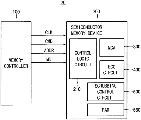
a memory cell array including a plurality of memory cell rows, each of the plurality of memory cell rows including volatile memory cells coupled to a plurality of bit-lines;
an error correction code (ECC) circuit;
a scrubbing control circuit configured to generate scrubbing addresses for performing a scrubbing operation on a first memory cell row from among the plurality of memory cell rows; and
a control logic circuit configured to:
control the ECC circuit such that the ECC circuit performs an error detection operation on a plurality of codewords of a plurality of sub-pages in the first memory cell row to count a number of error occurrences during a first interval in the scrubbing operation, and
determine a sub operation in a second interval in the scrubbing operation after the first interval based on the number of error occurrences in the first memory cell row,
wherein in the scrubbing operation, the control logic circuit is configured to control the scrubbing control circuit to generate the scrubbing addresses with a second period smaller than a first period determined in a specification of the semiconductor memory device during an initial interval after a power is applied to the semiconductor memory device, and
wherein the initial interval is a predetermined interval.
|