| CPC G11C 16/24 (2013.01) [G11C 7/12 (2013.01); G11C 11/005 (2013.01); G11C 16/0483 (2013.01); H10B 41/20 (2023.02); H10B 41/35 (2023.02)] | 20 Claims |

|
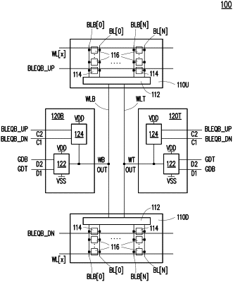
1. A memory circuit comprising:
first and second memory segments;
first and second write lines coupled to each of the first and second memory segments;
a first write line circuit coupled to the first write line and configured to receive first and second data signals; and
a second write line circuit coupled to the second write line and configured to receive the first and second data signals,
wherein
the memory circuit is configured to:
cause the first and second data signals to have complementary low and high logical states during a write operation to the first or second memory segment, and
cause each of the first and second data signals to have the low logical state during a masked write operation to the first or second memory segment, the first write line circuit is configured to:
output, to the first write line, a first write line signal responsive to the first data signal during the write operation, and
float the first write line during the masked write operation, and the second write line circuit is configured to:
output, to the second write line, a second write line signal responsive to the second data signal during the write operation, and
float the second write line during the masked write operation.
|