| CPC G09G 3/3225 (2013.01) [G09G 3/3233 (2013.01); G09G 3/3275 (2013.01); H10K 50/865 (2023.02); H10K 59/121 (2023.02); H10K 59/1213 (2023.02); H10K 59/1216 (2023.02); H10K 59/131 (2023.02); H10K 59/351 (2023.02); H10K 59/65 (2023.02); H10K 59/88 (2023.02); H10K 71/00 (2023.02); H10K 71/621 (2023.02); G09G 2300/0413 (2013.01); G09G 2300/0426 (2013.01); G09G 2300/0819 (2013.01); G09G 2300/0842 (2013.01); G09G 2310/0272 (2013.01); G09G 2310/08 (2013.01); H10K 59/1201 (2023.02); H10K 59/353 (2023.02)] | 20 Claims |

|
1. A display panel, comprising:
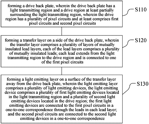
a drive back plate having a light transmitting region and a drive region at least partially surrounding the light transmitting region, wherein the drive region has a plurality of pixel circuits and at least comprises first pixel circuits and second pixel circuits;
a transfer layer provided on a side of the drive back plate and comprising a plurality of layers of mutually insulated lead layers, wherein each of the lead layers comprises a plurality of mutually insulated leads, and each lead extends from the light transmitting region to the drive region and is connected to one of the first pixel circuits; and
a light emitting layer provided on a side of the transfer layer away from the drive back plate and comprising a plurality of light emitting devices, wherein the light emitting device comprises a plurality of first light emitting devices located in the light transmitting region and a plurality of second light emitting devices located in the drive region, wherein:
the first light emitting devices are connected to the first pixel circuits in a one-to-one correspondence through the leads in each lead layer, and the second pixel circuits are connected to the second light emitting devices in a one-to-one correspondence;
the light emitting device comprises: a first electrode provided on a surface of the transfer layer away from the drive back plate, and the first electrode has an electrode portion and a wiring portion located outside an edge of the electrode portion;
each of the first electrodes is connected to one of the leads through the wiring portion and a transfer hole in the transfer layer, a light emitting function layer is provided on a surface of the first electrode away from the drive back plate, and a second electrode is provided on a surface of the light emitting function layer away from the drive back plate;
a plurality of layers of the lead layers at least comprises a first lead layer, a second lead layer, and a third lead layer that are sequentially distributed from the drive back plate to the light emitting layer, a lead of the first lead layer comprising a first lead, a lead of the second lead layer comprising a second lead, and a lead of the third lead layer comprising a third lead; and
a region of the transfer layer corresponding to the light emitting region comprises a plurality of routing regions distributed in an array, each of the routing regions comprises a target routing region, the target routing region is located at a side of a first central axis, and the target routing region comprises a first sub-region, a second sub-region, a third sub-region sequentially distributed towards the first central axis along a row direction, the first central axis being a central axis of the light transmitting region along a column direction.
|